


Research
1. Photonic nanowires (since fall 2006)
| In October 2006 profs. Weman and Fimland initiated a project on the growth and fabrication of GaAs based nanowires grown by Au-catalyzed molecular beam epitaxy (MBE). Structural properties are studied by TEM, SEM, XRD and AFM. Optical properties of individual nanowires will be studied by low temperature micro photoluminescence, as well as by nano-optical techniques using scanning confocal microscopy and scanning near-field optical microscopy. The long term goal is to process single nanowires into different photonic devices like nanowire emitters (LEDs, lasers) and detectors. Since 2007 this project is also supported by the Norwegian Research Council's "NANOMAT" program. This project is done in collaboration with Dr. Harmand at the Laboratory of Photonics and Nanostructures, CNRS, France and Prof. P.O. Holtz at the Division of Materials Science, Linköping University, Sweden. |

Fig.1. Schematic drawing of the Au-catalytic VLS growth of a single GaAs nanowire.

Fig.2.
Scanning electron microscope image of first GaAs nanowire grown at NTNU.
| The main objective of this project is to establish an improved understanding of organic/inorganic interfaces and to engineer interfaces that promote efficient organic/inorganic solar cells. The inorganic planar and nanostructured (nanorods/nanowires) oxide thin films (ZnO and other oxides) will be grown by by pulsed laser deposition (PLD). This project is done in close collaboration with SINTEF Materials and Chemistry (Trondheim, Norway) and Prof. R. Collins at the Center for Solar and Electronic Materials at the Colorado School of Mines, USA and is supported by the Norwegian Research Council. |
3. Photonic quantum-wires (since 1996 with EPFL, Switzerland)
|
Since 1996 I have been collaborating with Prof. Eli Kapon at the
Laboratory of Physics of Nanostructures, Swiss
Federal Institute of Technology in Lausanne (EPFL), on the investigation of
a number of novel V-groove quantum wire (QWR) devices including QWR
LEDs and lasers, absorption in QWR waveguide modulators, tunneling
between coupled double QWR LEDs, as well as high magnetic field studies
of such devices.
The high-quality InGaAs/AlGaAs V-groove quantum wires are made by self-ordering effects during metalorganic chemical vapor-phase deposition growth on V-grooved GaAs substrate. Some of these projects are summarized briefly below. |
|
Quantum wire
LEDs and
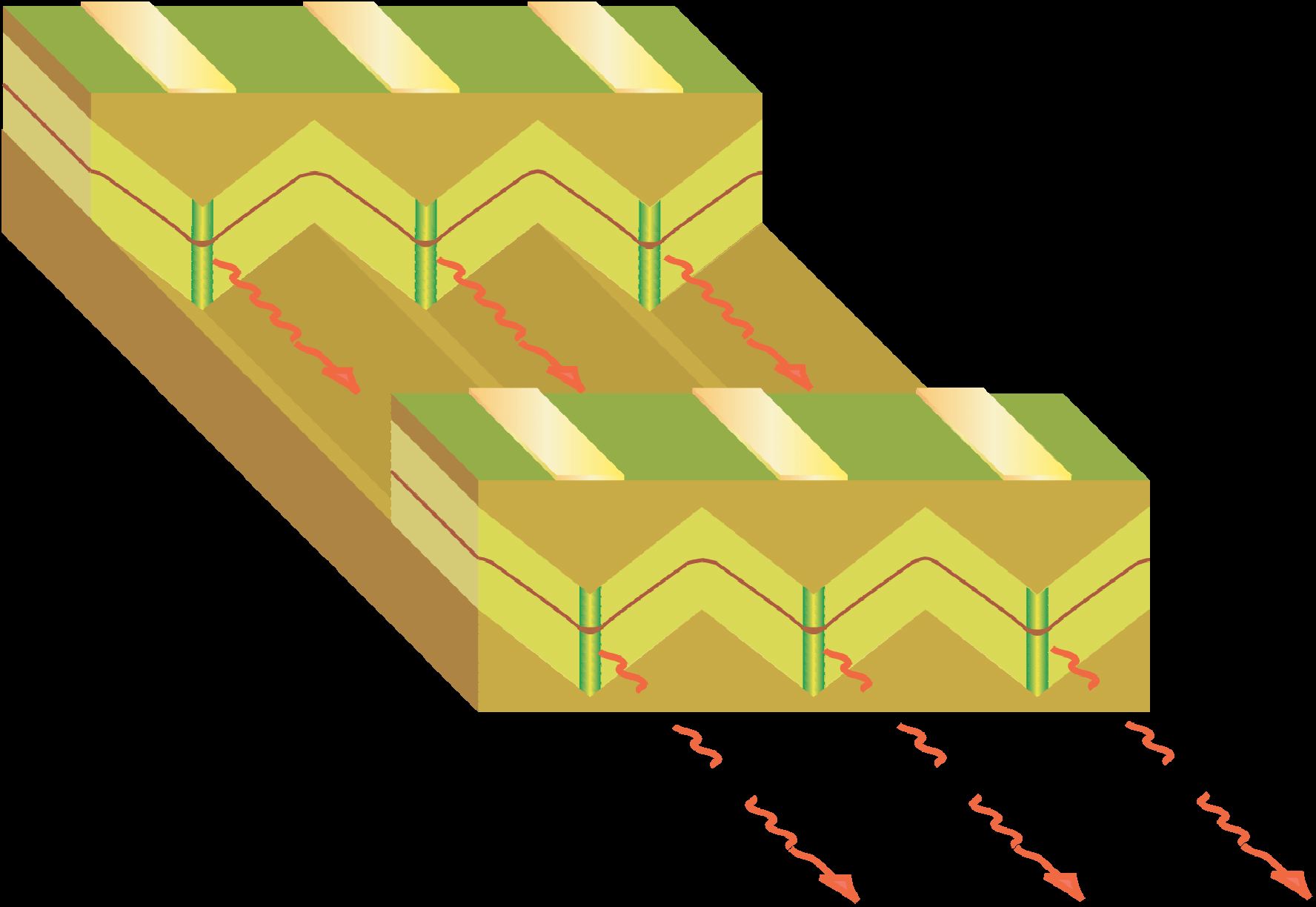
lasers The QWRs are using a unique way of selectively injecting charge carriers into the active V-groove QWRs via self-ordered vertical quantum wells. This has allowed us to develop novel LEDs exhibiting high internal quantum efficiencies with very narrow linewidth electroluminescence from 1D excitons at room temperature. We also study QWRs in deep V-grooves (3 um pitch), in order to investigate if selective current injection can be obtained together with a V-shaped dielectric waveguide. This would have very important implications for obtaining very low threshold current QWR laser diodes. |
|
|
Quantum wire modulators Here we study V-shaped semiconductor electro absorption modulators with V-groove QWRs in the active medium. Electro-absorption modulation is investigated by a combination of the quantum confined Stark effect and phase-space absorption quenching. We characterize these small waveguide modulators by measuring the electro-absorption by a combination of near- and far-field micro-optical techniques. We believe these modulators have the potential for high speed, low-voltage operation and compact size necessary for the next-generation optical networks. |
|
|
Coupled quantum wires
Optical
devices based on nanostructures such as QWRs, normally consist of stacked
layers in order to enhance the active volume. Knowledge about the
carrier transfer between QWRs is thus important since the optical
properties will be affected by how the injected carriers are
distributed among the different wires.
We have found that the carrier transfer is more efficient between quantum wells, despite a
higher tunneling barrier compared with the QWRs. The transfer between
the QWRs is well explained by tunneling, while the transfer between the
quantum wells must be explained by alternative mechanisms.
|


Editor: Helge Weman, Last updated: May 11, 2007